
Datoteka:MicroChipAtomicTrap00.jpg

Vidi sliku u punoj veličini (890 × 976 piksela, veličina datoteke: 44 KB, MIME tip: image/jpeg)
| Ova je datoteka sa Zajedničkog poslužitelja i mogu je rabiti drugi projekti. Opis s njezine stranice s opisom datoteke prikazan je ispod. |
| Opis |
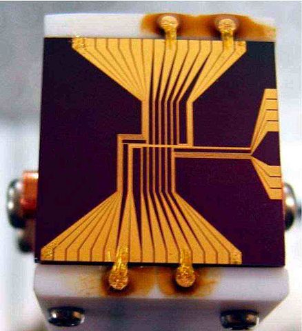
The first microchip atomic trap, designed at the Institute for Laser Science, Japan. The structure of wires is painted with gold at the insulator substrate. The main wire has Z-shape; the magnetic field allows the trapping of neutral atoms due to their magnetic momentum. The ship has sizes 2 x 2 cm. It was placed to the uniform magnetic field (source of this field is not shown in the figure); the traping is realized for so-called "atoms seeking for low magnetic field". The only atoms with positive spin-field energy were trapped. The miminim of the field is realized at the side of the chip, close to the central part of the z-electrode with electric current. This movement is limited by the edges of the "Z". Additional electrodes were designed to allow the play with the effective potential along this wire; the interaction with laser beams and reduction of the trapping potential allow the additional cooling of atoms (coling with vaporation), reaching the BEC. In the current design, the only one additional electrode is supplied with contacts. It was planned to use other electrodes to modify the potential in experiments with single-dimentional quantum mechanics. Actually, more advanced microchip atomic traps were manufactured instead. |
| Datum | y.2003 |
| Izvor | private communication |
| Autor | Ken-Ichi Nakagawa |
| Dopuštenje (Naknadna uporaba ove datoteke) |
copuleft directly from author |
| Ostale inačice |
Up to my knowkedge, it is the best resolution image of the First Microship Atomic Trap, ever posted. lower resolution pics are available at
|

|
Nositelj autorskog prava na ovoj datoteci dopušta svakome rabiti je za svaku svrhu, pod uvjetom da je nositelj autorskog prava propisno imenovan. Raspačavanje, izvedena djela, komercijalna uporaba, i svaka druga uporaba dozvoljeni su. |
|
|
Links
Povijest datoteke
Kliknite na datum/vrijeme kako biste vidjeli datoteku kakva je tada bila.
| Datum/Vrijeme | Minijatura | Dimenzije | Suradnik | Komentar | |
|---|---|---|---|---|---|
| sadašnja | 05:47, 12. rujna 2007. | | 890 × 976 (44 KB) | Domitori | {{Information |Description=The first microchip atomic trap, designed at Institute for Laser Science, Japan. The main wire has Z-shape; the magnetic field allows the trapping of neutral atoms due t |
Uporaba datoteke
Na ovu sliku vode poveznice sa sljedećih stranica:
Globalna uporaba datoteke
Sljedeći wikiji rabe ovu datoteku:
- Uporaba na en.wikipedia.org
- Uporaba na es.wikipedia.org
- Uporaba na fa.wikipedia.org
- Uporaba na fr.wikipedia.org
- Uporaba na he.wikipedia.org
- Uporaba na it.wikipedia.org